PRODUCT DESIGN & DEVELOPMENT SERVICES
End-to-End Product Design & Development Solutions
Product Design & Development
From concept engineering to production-ready hardware, BU Labs helps startups, OEMs, and R&D teams accelerate innovation with high-performance electronic product design services.
Our engineering-driven development approach combines advanced schematic design, PCB engineering, prototyping, validation, and system optimization to reduce development cycles, improve reliability, and speed up time-to-market.
- High-Speed Schematic Design
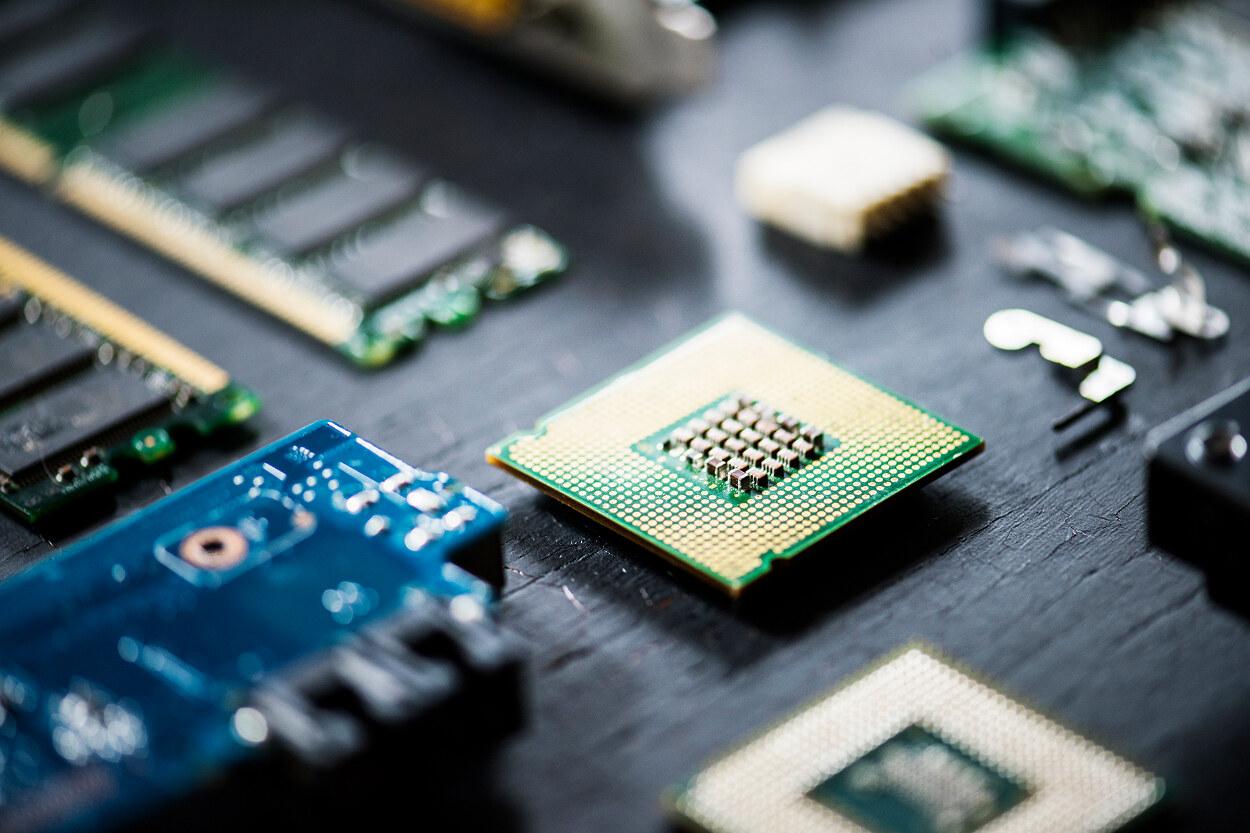
- Advanced PCB Design (RF, SI, High-Speed)
- FPGA & ASIC Validation Boards
- Embedded Hardware Architecture
- ASIC Validation Boards
- Prototype Development & Bring-Up
- Functional Testing & Debugging
- Design Optimization for Manufacturing (DFM)
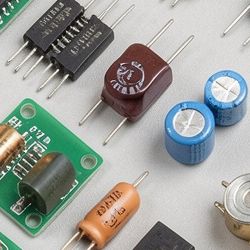
- Component Selection & BOM Engineering
- Product Validation & Reliability Testing
Who We Support
We partner with hardware startups, semiconductor companies, OEMs, embedded system developers, and industrial R&D teams building next-generation electronic products.
Whether you are developing a proof-of-concept, validating a new hardware platform, or preparing for scalable production, BU Labs provides integrated engineering support across the complete product development lifecycle.
WHAT WE DELIVER
From architecture planning and prototype validation to optimized PCB design and product readiness, BU Labs delivers scalable hardware engineering solutions that help organizations innovate faster and reduce development complexity.
Our team focuses on building reliable, manufacturable, and production-ready electronic systems tailored for high-performance applications.
Design & System Architecture
PCB Design & Hardware Bring-Up
Prototype & Functional Validation
Performance Optimization & Scalability
BU Labs
HOW WE WORK
From concept to production readiness, we follow a structured engineering workflow that minimizes redesign effort, accelerates validation, and improves product reliability.
Our integrated execution model combines hardware architecture, PCB engineering, prototyping, testing, and optimization into a seamless development process — enabling faster innovation cycles and reduced time-to-market.
- Design architecture and engineering planning
- Prototype development and functional validation
- High-speed PCB design and system bring-up
- Optimization for scalability and production readiness
Why us
Why Choose BU LABS for Product Design & Development?
We help engineering teams accelerate innovation with scalable, high-performance hardware development solutions.
End-to-End Hardware Development
From idea to validated prototype, we manage the complete hardware product development lifecycle under one engineering ecosystem.
Faster Product Development Cycles
Integrated design, prototyping, and validation workflows reduce delays and accelerate product launches.
Advanced PCB Engineering Expertise
Expertise in RF, SI, high-speed, and multilayer PCB design for complex electronic systems.
Prototype-to-Production Readiness
We design systems optimized for validation, manufacturability, scalability, and long-term reliability.
Flexible Engineering Engagements
Support models tailored for startups, OEMs, and enterprise R&D teams — from project-based execution to dedicated engineering support.
Bengaluru-Based Engineering Team
On-ground execution and engineering collaboration from India’s growing electronics and hardware innovation hub.